Here is my layout for a DDNF I/V Buffer PSU.
On the left a standard PSU for the +15V and on the right a symmetrical psu for the +/- 19V.
All lines are designed for the Mundorf M-LYTIC AG+ 4-Pole caps.
If you want to use normal 2-Pole Snap-In caps, just short the pads.
Just an idea...


BTW, I have attached a interesting "4-pin vs. 2-pin Caps" document from Mundorf.
On the left a standard PSU for the +15V and on the right a symmetrical psu for the +/- 19V.
All lines are designed for the Mundorf M-LYTIC AG+ 4-Pole caps.
If you want to use normal 2-Pole Snap-In caps, just short the pads.
Just an idea...
An externally hosted image should be here but it was not working when we last tested it.
An externally hosted image should be here but it was not working when we last tested it.
BTW, I have attached a interesting "4-pin vs. 2-pin Caps" document from Mundorf.
Attachments
If there is enough request to start a GB, i will send the 1st sample to Pedja for testing.
Hi Oliver
I would take at least 2 modules of Pedja Rogic DDNF I/V.
Best regards
Help with TDA1541A Signal Voltages
Hello All,
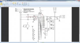
I am building the TDA1541A dvb-Projekt board, v2.3, and I am having some difficulties in determining why the signal levels are very low on BCLK. I have attached the diagram from Oliver's schematic with some points marked A to J. I would very much appreciate if someone could scope those points and tell me what the peak-to-peak voltages are?
The signals from the Teralink are all coming in at about 5V p-p, so there doesn't seem to be an issue there. I have tried shorting the inductor and that did not help. Here are the input signal levels I am seeing:
Pin 1: 44.1KHz, 740mV p-p
Pin 2: 2.82MHz, 424mV p-p
Pin 3: Data
Pin 4: same as pin 2
I also have all the other pin DC voltages. I have done the mods on the PCB, feeding the Salas shunt regulators directly in to where the TL431 regulators were. At the IC pins, I am getting exactly -5V, +5V and -15V.
Any help would be appreciated! Thank you!
Gary
Hello All,
I am building the TDA1541A dvb-Projekt board, v2.3, and I am having some difficulties in determining why the signal levels are very low on BCLK. I have attached the diagram from Oliver's schematic with some points marked A to J. I would very much appreciate if someone could scope those points and tell me what the peak-to-peak voltages are?
The signals from the Teralink are all coming in at about 5V p-p, so there doesn't seem to be an issue there. I have tried shorting the inductor and that did not help. Here are the input signal levels I am seeing:
Pin 1: 44.1KHz, 740mV p-p
Pin 2: 2.82MHz, 424mV p-p
Pin 3: Data
Pin 4: same as pin 2
I also have all the other pin DC voltages. I have done the mods on the PCB, feeding the Salas shunt regulators directly in to where the TL431 regulators were. At the IC pins, I am getting exactly -5V, +5V and -15V.
Any help would be appreciated! Thank you!
Gary
Attachments
Hi Gary,
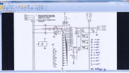
attached the voltages pp from A to J.
You repoted that the DC voltage on the lower side of the 10mH inductor are 4.75V.
That´s curious. The voltage must be stable +5V from the injection (TL431 pin) to Pin14 of the 74HC02.
Perhaps it would help if you post some detailed pictures for an overview.
Best,
Oliver
Attachments
Layout and PCB Pictures - TDA1541A v2.3
Hi Oliver -
Thank you for taking time from your schedule to assist me. By the numbers you have given, it looks like SCLK is just a little low - you measure about 1 Vpp, I measured 0.760Vpp. This is about the same proportion on BCLK.
I've attached 2 pictures of the PCB and layout. Just for quick testing, I'm using a couple of 47 ohm resistor to ground from the current outputs. They're connected from GND to the red/black wires that go to the master slave. This is actually the upper PCB of the 2 that I will use, set up for testing on this issue. If you're curious about the I/V resistors, I am doing the conversion on the tube out PCB.
I've also attached a scope shot. The picture shows the BCLK on the OUT side of the resistor that is CLOSER to the electrolytic capacitor (either R21 or R22?) This waveform looks very bad. Does yours appear the same? Or it does not matter going into the Cosc pins?
BTW - The voltage I mentioned previously on the bottom side (toward the TDA1541) of the inductor should be lower - it has a DC resistance so there should be some drop. I provided that to perhaps compare what you were seeing. Are you not getting about 250mV drop? It has a 23.8 ohm resistance, meaning about 10.5mA of current were flowing into the Pin 1 node. does that seem high?
Thank you,
Gary
Last edited:
Hi Oliver -
Thank you for taking time from your schedule to assist me. By the numbers you have given, it looks like SCLK is just a little low - you measure about 1 Vpp, I measured 0.760Vpp. This is about the same proportion on BCLK.
I've attached 2 pictures of the PCB and layout. Just for quick testing, I'm using a couple of 47 ohm resistor to ground from the current outputs. They're connected from GND to the red/black wires that go to the master slave. This is actually the upper PCB of the 2 that I will use, set up for testing on this issue. If you're curious about the I/V resistors, I am doing the conversion on the tube out PCB.
I've also attached a scope shot. The picture shows the BCLK on the OUT side of the resistor that is CLOSER to the electrolytic capacitor (either R21 or R22?) This waveform looks very bad. Does yours appear the same? Or it does not matter going into the Cosc pins?
BTW - The voltage I mentioned previously on the bottom side (toward the TDA1541) of the inductor should be lower - it has a DC resistance so there should be some drop. I provided that to perhaps compare what you were seeing. Are you not getting about 250mV drop? It has a 23.8 ohm resistance, meaning about 10.5mA of current were flowing into the Pin 1 node. does that seem high?
Thank you,
Gary
Gary,
you short the Iout lines (I/V-Resistors on the PCB) to ground.Remove the two bridges and you got your missing signal. I think that´s it...
Gary,
I think there are a couple of things you should do:
1. Get the logic levels corrected.
2. Improve the wiring.
1: You are not getting the correct logic levels because you have some resistors to GND. I have not followed the whole thread, I just got here from this thread:
http://www.diyaudio.com/forums/digi...04-transceiver-module-tda1541a-problem-2.html
I assume that you want a 5V logic level on the DAC. If this is the case you should remove R31, R30, R29 and the three pull up resistors connected to F, G and H (I cannot read the resistor numbers or values).
The resistor values for R3 and R5 are perhaps a bit too high and may limit the slew rate and distort the digital data.
If the input is 5V logic and you need e.g. 3.3V logic you could use the pull down resistors to get the right level. But right now the levels are reduced far too much (and should not be reduced at all if you want 5V logic levels).
I assume that the pull up and pull down resistors have been added in an attempt to "clean up" the logic signals. Which leads me to issue no. 2:
The wiring seems to be less than optimal. There is a big risk that you will see excessive ringing and distortion on the logic signals, perhaps enough to make the circuit stop working.
I suggest to use a flat cable where every second wire is connected to GND (at both ends) and the wires in-between are used for the BCK, FS and DATA signals. This will give a much better digital signal quality. You may then be able to remove most of the resistors in series (R4, R6, R7, R8 and R25) and perhaps just keep R25.
I have seen a similar issue with an I2S signal to a DAC. Initially it wouldn't work. When I connected it with a flat cable as described the digital signals looked much better on the oscilloscope and the circuit worked!
1: You are not getting the correct logic levels because you have some resistors to GND. I have not followed the whole thread, I just got here from this thread:
http://www.diyaudio.com/forums/digi...04-transceiver-module-tda1541a-problem-2.html
I assume that you want a 5V logic level on the DAC. If this is the case you should remove R31, R30, R29 and the three pull up resistors connected to F, G and H (I cannot read the resistor numbers or values).
The resistor values for R3 and R5 are perhaps a bit too high and may limit the slew rate and distort the digital data.
If the input is 5V logic and you need e.g. 3.3V logic you could use the pull down resistors to get the right level. But right now the levels are reduced far too much (and should not be reduced at all if you want 5V logic levels).
I assume that the pull up and pull down resistors have been added in an attempt to "clean up" the logic signals.
Hi Jens,
i appreciate that you would help to find Gary´s failure, but as you wrote you don´t know the circuit you are talking about.
R3, R5 & R26-R31 are part of -ecdesigns- I2S attenuator
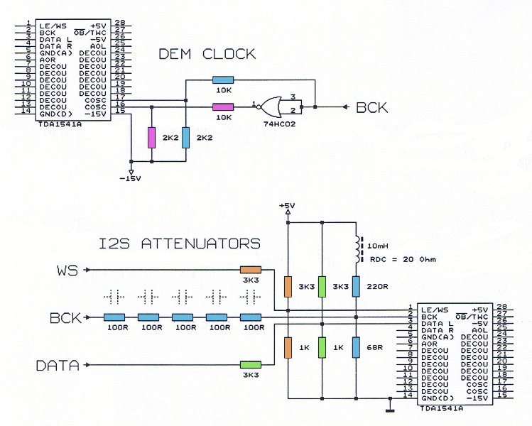
and not part of the problem why Gary has no sound output!
Oliver,
Sometimes the obvious...is not OBVIOUS. Thank you for pointing that out. Not sure what I was thinking when I did that.
Here's what I have done so far:
1 - Remove those wires on the I/V
2 - I fixed the logic levels in the Teralink. I had a zener reference in there, which I was using before I did the shunt power supply. This was causing the logic levels to be a little lower than yours, now they are the same as you have on A to J.
3 - I put a new TDA1541A chip in
4 - It's still no signal!!!
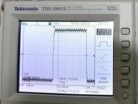
The only odd thing I can see is the FCLK signal looks a little noisy on the flats, I have attached a picture. Does your signal have a similar noise?
ALSO: With the chip out of the socket, and my temporary I/V resistors in place, I checked the resistance from the AOL and AOR pins on the socket, and I was getting 50 ohms.
Thanks,
Gary
Sometimes the obvious...is not OBVIOUS. Thank you for pointing that out. Not sure what I was thinking when I did that.
Here's what I have done so far:
1 - Remove those wires on the I/V
2 - I fixed the logic levels in the Teralink. I had a zener reference in there, which I was using before I did the shunt power supply. This was causing the logic levels to be a little lower than yours, now they are the same as you have on A to J.
3 - I put a new TDA1541A chip in
4 - It's still no signal!!!
The only odd thing I can see is the FCLK signal looks a little noisy on the flats, I have attached a picture. Does your signal have a similar noise?
ALSO: With the chip out of the socket, and my temporary I/V resistors in place, I checked the resistance from the AOL and AOR pins on the socket, and I was getting 50 ohms.
Thanks,
Gary
Attachments
Last edited:
JensH;
Thank you for helping out.
This project has been used in the same way be I think, quite a few (maybe hundreds?) DIY's and seems to be working so far. Yes, my wiring looks a bit messy but this is pretty low frequency stuff and it will be cleaned up once it's in the chassis. I'm just trying to get it working right now!
Gary
Gary,
I think there are a couple of things you should do:
1. Get the logic levels corrected.
2. Improve the wiring.
1: You are not getting the correct logic levels because you have some resistors to GND. I have not followed the whole thread, I just got here from this thread:
http://www.diyaudio.com/forums/digi...04-transceiver-module-tda1541a-problem-2.html
I assume that you want a 5V logic level on the DAC. If this is the case you should remove R31, R30, R29 and the three pull up resistors connected to F, G and H (I cannot read the resistor numbers or values).
The resistor values for R3 and R5 are perhaps a bit too high and may limit the slew rate and distort the digital data.
If the input is 5V logic and you need e.g. 3.3V logic you could use the pull down resistors to get the right level. But right now the levels are reduced far too much (and should not be reduced at all if you want 5V logic levels).
I assume that the pull up and pull down resistors have been added in an attempt to "clean up" the logic signals. Which leads me to issue no. 2:
The wiring seems to be less than optimal. There is a big risk that you will see excessive ringing and distortion on the logic signals, perhaps enough to make the circuit stop working.
I suggest to use a flat cable where every second wire is connected to GND (at both ends) and the wires in-between are used for the BCK, FS and DATA signals. This will give a much better digital signal quality. You may then be able to remove most of the resistors in series (R4, R6, R7, R8 and R25) and perhaps just keep R25.
I have seen a similar issue with an I2S signal to a DAC. Initially it wouldn't work. When I connected it with a flat cable as described the digital signals looked much better on the oscilloscope and the circuit worked!
Oliver,
Thanks for the schematic. Now I can see what is going on! Interesting way of doing things, but not exactly standard practice.
I do think that this circuit is part of the problem though. With very low voltage swing on the digital lines there is a big risk that the signals do not represent valid logic signals to the inputs of the IC. The logic threshold on the inputs can vary from one device to another (and with emperature) and with a very small difference between high and low level there is a risk that the input(s) will see the signal as being either high or low all the time. With proper logic levels there is usually a good margin. With this circuit there is no guarantee that it will actually work.
I suggest to try my initial proposal first to get things working. Then perhaps modifications can be made later, one at a time.
I am not convinced that the I2S attenuator will improve the sound though. I would start by making sure the wiring is correct and that ringing and overshoot etc. on the digital signal lines is eliminated.
Oliver,
Thanks for the schematic. Now I can see what is going on! Interesting way of doing things, but not exactly standard practice.
I do think that this circuit is part of the problem though.....With this circuit there is no guarantee that it will actually work.
You do realise that this circuit has been tested to work, not only functionally, but spectacularly, numerous times.
Gary, I think the first thing you should do is to check the voltages on the actual TDA1541A chip itself. If all are present, then your problem is either the chip, the output stage or the input stage, but voltages are best to check first.
If all Vdc are present and correct on the right pins, then next check the presence of the digital signal (Hz) on the chip itself. If all present and correct, then check the output signal. That's what I found useful when I had a no sound board. In my case it was a blown inductor on the board (a brand new component).
Good Luck!
Lucas
Lucas,
My voltages are set right at the chip pins: -5V, +5V, and -15V. I am getting proper FS/FCLK (1Vpp), BCLK(0.5Vpp) and DATA at the chip pins. I am using a 1KHz test tone into the USB. I think BCLK is a bit low, but Oliver confirmed his is about that level as well. I have checked the inductor by shorting it out. No difference.
There is no sine output, just noise...not sure where to go next. It's certainly not the chips either, I have quite a few and have swapped them.
BTW - I am just using a pair of 50 ohm resistors from AOL/AOR to GND for testing at this point and looking for a sine signal on them
Thanks,
Gary
Last edited:
Good advice from Lucas. Also even though this won't help you get your sound, but will help it sound better once you do. You need to shorten the wires coming from the salas shunts to the tl431 pin holes. They are way too long at present. Get them as short as you possibly can(less then 10cm).
Also where are your decoupling caps around the tda1541a chip?
Also where are your decoupling caps around the tda1541a chip?
Yes, I will shorten the wires once I get it working in some form, and once it's in the chassis. I cannot imagine that longer wires are stopping the analog outputs from working...
For decoupling, I'm using Panasonic 1206 series SMC film caps 0.47uf/16V, right on the bottom side pins. I've verified they are all making proper connection with no shorts.
Question: Have both you and Lucas made this board?
BTW - thank you to all who are helping me out with this frustrating problem!
Gary
Last edited:
Hi Gary, yes both Lucas and I have made this board and both of us also had no sound at first!!! So totally understand your frustration. Yes don't think my suggestion will get you sound, just will make it sound better once you do get it up and running.
What are you using for your output stage?
What are you using for your output stage?
Hi,
Right now - I am using just 50 ohm resistors to ground to see if I can just get a voltage sine wave. Although it will be small, I should be able to see it. However, I have measured DC voltages at the AOL and AOR pins and something odd - they are both at -103mV. That does not seem correct, I thought these pins must be at 0V in order to work correctly. Why would I get this voltage at those pins?
Also, can you tell me at what point (where) you tie the DGND and the AGND together from the TDA1541A PCB?
Can I ask a big favor? Can you measure the DC voltages at each of the pins so I can compare to mine? I think this would help out. Thank you!
Gary
Last edited:
- Status
- This old topic is closed. If you want to reopen this topic, contact a moderator using the "Report Post" button.
- Home
- Group Buys
- "Reference" TDA1541A DAC with I2S-BUS architecture