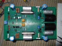
Just finished my main PCB according Salas instructions.
I attached files for main, copper and silkscreen in PDF format.
Right now I gonna prepare my self to etch my first PCB.
Nice work !
Please post some pictures of the pcb (after you etch them).
Nice work !
Please post some pictures of the pcb (after you etch them).
Yes, it looks good.
But a comment to the grounding: afaik it is not good to change from wide traces to narrow traces and vice versa.
Specially not when currents are flowing, what is the case for the grounding, specially between the bypass caps.
Franz
/Edit: try to explain (afaik): different size of traces is resulting in minimal differences of conducitvity eg. resistance. When currents are flowing this will produce voltage differences on the grounding traces. And this is to be avoided. Better use one trace width, as large as possible.
Last edited:
BOS might be even better than NOS
Everything depends on the burning.
The burning was doing with 1st quality wood (ebony) & slow fire to cook the cap as better as possible.

@NPower
In your pcb I don't like IN gnd + RL gnd not referred with thier own track to star gnd. If you connect them to D4 gnd and R2V gnd, you mix up Signal gnd and Power gnd. Not good at all.
Take example from OUT gnd and R8 gnd: correct routing.
Plenty of space to fix this problem....
In your pcb I don't like IN gnd + RL gnd not referred with thier own track to star gnd. If you connect them to D4 gnd and R2V gnd, you mix up Signal gnd and Power gnd. Not good at all.
Take example from OUT gnd and R8 gnd: correct routing.
Plenty of space to fix this problem....
You did not forget the garlic did you ?
I forgot thanks for advice I will do "a la llauna" catalan typical foot

Cod (bacalao), not snails, I hope!
Nice typo: catalan typical foot
Some of those are now on TV.... vs Switzerland!
Cod of course.
You see
I knew it before...
Congratulations Franz.
- Home
- Source & Line
- Analogue Source
- Simplistic NJFET RIAA