digikey transistors for i/v
can anyone help me
I am about to place an order with Digikey for various parts to build a D14T using Johns original project boards, and would like to know what alternative transistors to the Toshiba 2SC2240 can be ordered from Digikey.
I can get standard type transistors from Maplins locally over the counter, however I did not want to miss an opportunity to get some higher specification parts if they are stocked by Digikey.
here is a list of the toshiba ones stocked by Digikey
http://search.digikey.com/scripts/DkSearch/dksus.dll?Selection
here is a list of all Bipolar Transistors
http://search.digikey.com/scripts/DkSearch/dksus.dll?Cat=1376376&keywords=bipolar transistors
I just dont know where to start.
any ideas?
Builder Brad -
If you can't find equivalents at Digikey, you can get the 2SC2240 here: http://www.littlediode.com/components/home.php
If you can't find equivalents at Digikey, you can get the 2SC2240 here: http://www.littlediode.com/components/home.php
Hi Builder Brad,
http://www.cricklewoodelectronics.c...?cat=178&sort=orderby&sort_direction=0&page=6
It's best to put multiple (matched) transistors in parallel. I currently use 4 x 2SC2240 in parallel for both T1 and T2.
Transistor arrays like the MAT04 (4 x matched NPN transistor) from Analog Devices can also be used. Using one of the transistors for 0.6V reference voltage, and the other 3 for T1, will guarantee very low DC offset voltage at the TDA1541A output.
I can get standard type transistors from Maplins locally over the counter, however I did not want to miss an opportunity to get some higher specification parts if they are stocked by Digikey.
http://www.cricklewoodelectronics.c...?cat=178&sort=orderby&sort_direction=0&page=6
It's best to put multiple (matched) transistors in parallel. I currently use 4 x 2SC2240 in parallel for both T1 and T2.
Transistor arrays like the MAT04 (4 x matched NPN transistor) from Analog Devices can also be used. Using one of the transistors for 0.6V reference voltage, and the other 3 for T1, will guarantee very low DC offset voltage at the TDA1541A output.
Hi all,
D1 project update,
Yesterday I tested various DEM clock frequencies and phase (using the new differential DEM clock circuit with only 4 resistors) using the D1 prototype. I used a miniature rotary switch and a switch to reverse DEM clock polarity. I tested with both low level recordings (-40 ... -70dB), and high-quality recordings (Stockfish).
Sound quality appears to increase with DEM clock frequency, and I settled for 2.8224 MHz. I couldn't use these high frequencies with the previous differential DEM clock as the circuit wasn't stable, now using the 4 resistors, it's no problem at all.
It seems that DEM clock phase is also important:
Non-inverted DEM clock goes to pin 17, inverted DEM clock goes to pin 16. Non-inverted means that the DEM clock signal = bit clock, or divided bit clock using a divider that triggers on the positive going edge of the bit clock.
Also some news from the SD-player project, yesterday I listened to lossless music (44.1/16) originating from the SD-card player prototype
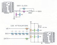
I attached latest DEM clock and I2S attenuator schematics. The I2S attenuators can also be used for the TDA1543.
The DEM clock circuit consists of two resistive attenuators that perform biasing, level-shifting and attenuation. The DEM clock frequency has been increased to 2.8224 MHz (bit clock).
The I2S attenuators provide both a bias voltage (approx. 1.2V), and attenuation of the I2S signals. By lowering I2S signal amplitude, sound get's much more refined, due to reduction of I2S interference.
The bit clock (BCK) attenuator needs a choke (10mH Panasonic ferrite-core choke) to attenuate power supply noise. This choke will also provide a high impedance to +5V, so the series resistor value can be increased, and the shunt resistor value can be lowered.
I used multiple 100R resistors in order to minimize the effect of resistor stray capacitance.
I tried many, more complicated discrete designs. This simple circuit performs best so far, especially when using multiple low noise transistors in parallel, minimizing current flow through each transistor.
The simple trans-impedance I/V converter uses current steering and is extremely fast (large bandwidth). By using few high quality (low noise) parts, signal degradation can be minimized.
Single-ended output (class A) seems to provide cleanest sound, as cross-over distortion is eliminated.
The DEM clock circuit consists of two resistive attenuators that perform biasing, level-shifting and attenuation. The DEM clock frequency has been increased to 2.8224 MHz (bit clock).
The I2S attenuators provide both a bias voltage (approx. 1.2V), and attenuation of the I2S signals. By lowering I2S signal amplitude, sound get's much more refined, due to reduction of I2S interference.
The bit clock (BCK) attenuator needs a choke (10mH Panasonic ferrite-core choke) to attenuate power supply noise. This choke will also provide a high impedance to +5V, so the series resistor value can be increased, and the shunt resistor value can be lowered.
I used multiple 100R resistors in order to minimize the effect of resistor stray capacitance.
I am a little confused. I have been trying out the transimpedance circuit until someone told me using the current conveyance with the output DC blocking cap is not the best.
Someone suggested diamond differential output. any comment.
I tried many, more complicated discrete designs. This simple circuit performs best so far, especially when using multiple low noise transistors in parallel, minimizing current flow through each transistor.
The simple trans-impedance I/V converter uses current steering and is extremely fast (large bandwidth). By using few high quality (low noise) parts, signal degradation can be minimized.
Single-ended output (class A) seems to provide cleanest sound, as cross-over distortion is eliminated.
Attachments
great news dear EC !
if you say it's the best DEM reclock circuit tested by you so far i believe you")
so you have used 74HC02 as an inverter for the inverted 2,8 mhz signal? is this the best logic that can be used in this application?
Also i would like to know your opinion on the posibility of using directly the inverted Masterclock from the KWAK CLOCK 7 obtained from pin 7 of the AD8561 comparator so this way an inverter wouldn't be needed any more.
Or is it better to obtain the inverted signal from the non-inverted one used for the BCK ?
My last question - do we need some extra buffer to drive the 2,8 mhz masterclock simultaneously to BCK and to the DEM clock inverter to minimise interference and jitter?
Thanks !
if you say it's the best DEM reclock circuit tested by you so far i believe you
so you have used 74HC02 as an inverter for the inverted 2,8 mhz signal? is this the best logic that can be used in this application?
Also i would like to know your opinion on the posibility of using directly the inverted Masterclock from the KWAK CLOCK 7 obtained from pin 7 of the AD8561 comparator so this way an inverter wouldn't be needed any more.
Or is it better to obtain the inverted signal from the non-inverted one used for the BCK ?
My last question - do we need some extra buffer to drive the 2,8 mhz masterclock simultaneously to BCK and to the DEM clock inverter to minimise interference and jitter?
Thanks !
Hi luxury54,
I just used this inverter for testing, doesn't seem to be very critical. It's also possible to use a single inverter, NAND, or NOR gate (Fairchild tiny logic series).
This should work fine, clock load is minimum (10K series resistors).
The DEM clock circuit load is minimal, so extra buffering doesn't seem to be required. But if other circuits require the master clock too (SPDIF receiver / reclocker), an extra clock buffer is required.
I use the un-buffered master clock output to drive the TDA154x (through 500R series resistor that's part of the attenuator)
The un-buffered master clock also drives a clock buffer through 1K series resistor. This clock buffer is used to drive the DEM clock, the microprocessor-based tracker, and the CS8416 SPDIF receiver.
so you have used 74HC02 as an inverter for the inverted 2,8 mhz signal? is this the best logic that can be used in this application?
I just used this inverter for testing, doesn't seem to be very critical. It's also possible to use a single inverter, NAND, or NOR gate (Fairchild tiny logic series).
Also i would like to know your opinion on the posibility of using directly the inverted Masterclock from the KWAK CLOCK 7 obtained from pin 7 of the AD8561 comparator so this way an inverter wouldn't be needed any more.
This should work fine, clock load is minimum (10K series resistors).
My last question - do we need some extra buffer to drive the 2,8 mhz master clock simultaneously to BCK and to the DEM clock inverter to minimise interference and jitter?
The DEM clock circuit load is minimal, so extra buffering doesn't seem to be required. But if other circuits require the master clock too (SPDIF receiver / reclocker), an extra clock buffer is required.
I use the un-buffered master clock output to drive the TDA154x (through 500R series resistor that's part of the attenuator)
The un-buffered master clock also drives a clock buffer through 1K series resistor. This clock buffer is used to drive the DEM clock, the microprocessor-based tracker, and the CS8416 SPDIF receiver.
-ecdesigns- said:Hi Builder Brad,
http://www.cricklewoodelectronics.c...?cat=178&sort=orderby&sort_direction=0&page=6
It's best to put multiple (matched) transistors in parallel. I currently use 4 x 2SC2240 in parallel for both T1 and T2.
Transistor arrays like the MAT04 (4 x matched NPN transistor) from Analog Devices can also be used. Using one of the transistors for 0.6V reference voltage, and the other 3 for T1, will guarantee very low DC offset voltage at the TDA1541A output.
Cheers John,
I will try with both the SC2240s and some MAT04 transistors.
great work on the DEM reclock.
You are giving us a lot to think about.
I am using the 74HC4040 chip to derive the 352khz DEM signal, this is then inverted by a 74HC04 chip, both signals are then reclocked by two spare inputs on one of the 74HC174 flip flops that I am using to reclock the i2s signals from my squeezebox.
I thought that reclocking both of the DEM signals improved things.
I will try your DEM scheme over the weekend.
Brad
Hi ccschua,
74HCT04 is ok, resistors must be 10K and 2K2, no other values.
For the DEM circuit, how about a 74HCT04. Can this work? I dont have 10k, but 12k. Do I need to increase the 2.2k to 2.7k?
74HCT04 is ok, resistors must be 10K and 2K2, no other values.
Hi!
Excuse me for my bad english but i would like to share with you some Tina simulations.
Now I am using a (single) TDA1541A DAC with this i/v converter:
http://img24.imageshack.us/img24/7556/graphic1z.jpg
Look at the DAC's output voltage variation!
Distortion is very low (if we can believe in Tina...).
http://img11.imageshack.us/img11/7223/graphic2j.jpg
If using single transistor...
The BD139 is better than the BC550 for i/v conversion, because:
BD139:
http://img19.imageshack.us/img19/638/bd139.jpg
BC550C
http://img17.imageshack.us/img17/3928/bc550c.jpg
Because lower BE resistance???
On every picture:
The left BD139 and the potmeter for adjusting the zero emitter voltage are just for testing purpose. 560pF's for output's filtering in the physical realisation.
So, the power transistor is better... Anyway I use heatsink for the BD's, for reducing thermal memory distortion. It would be better for all the transistors.
Feedbacks are welcome.
Istvan
Hi istipisti,
Thanks for sharing this information.
My personal experience is that connecting a single current source that supplies more than approx. 40uA is already highly problematic. This is caused by the fact that it has to remain stable within less than 60nA in order to prevent affecting LSB. In practice this gets increasingly difficult with increased bias current. When using say 2mA bias current with the TDA1541A, do realize that this already represents half of the 4mA full-scale current, and introduced errors (injected noise) could be accordingly, especially with low level information.
Current sources may be perfect in a simulation, but in practice there is significant (power supply) pollution present that's extremely difficult to reduce to required nV / nA region. The simple constant current sources, based on a JFET are far from perfect and output current still varies with power supply voltage fluctuations.
You can easily test this by attempting to tune TDA1541A bit errors by feeding an external constant current into the active divider decoupling pins, and these are only the 6 MSBs!
I always build real prototypes, this way all relevant variables can be taken into account, not only the ones entered in a simulator program.
I had best audible results without any filtering at all, but I use large bandwidth power amps with local feedback.
My trans-impedance converter design may seem too simple, and there is the obvious "urge" to add many more components in an attempt to improve performance. But more complicated circuits don't necessarily result in better perceived sound quality, as the number of variables (and possible errors) increase accordingly.
What looks good on the oscilloscope, spectrum analyzer or in simulations can still result in poor perceived sound quality.
In fact, even a single bipolar transistor is problematic in these designs (noise modulation).
I first thought it were thermal memory effects, but they are not, it's noise that increases with the current passing through the semiconductor. So when the current is modulated (audio signal), noise amplitude is modulated too. By using multiple (matched) semiconductors in parallel, current running through each transistor is reduced accordingly, and so will the modulated noise amplitude. This technique is already used in moving-coil pre-amps that have to handle very low signals.
If you study the schematic you will see that I use current steering, providing very high bandwidth (up to 100 MHz), this results in extreme low phase errors and perfect signal transients (fast and without the slightest ringing). Noise levels are also lowest from all designs I tested before.
Thanks for sharing this information.
My personal experience is that connecting a single current source that supplies more than approx. 40uA is already highly problematic. This is caused by the fact that it has to remain stable within less than 60nA in order to prevent affecting LSB. In practice this gets increasingly difficult with increased bias current. When using say 2mA bias current with the TDA1541A, do realize that this already represents half of the 4mA full-scale current, and introduced errors (injected noise) could be accordingly, especially with low level information.
Current sources may be perfect in a simulation, but in practice there is significant (power supply) pollution present that's extremely difficult to reduce to required nV / nA region. The simple constant current sources, based on a JFET are far from perfect and output current still varies with power supply voltage fluctuations.
You can easily test this by attempting to tune TDA1541A bit errors by feeding an external constant current into the active divider decoupling pins, and these are only the 6 MSBs!
I always build real prototypes, this way all relevant variables can be taken into account, not only the ones entered in a simulator program.
560pF's for output's filtering in the physical realisation.
I had best audible results without any filtering at all, but I use large bandwidth power amps with local feedback.
My trans-impedance converter design may seem too simple, and there is the obvious "urge" to add many more components in an attempt to improve performance. But more complicated circuits don't necessarily result in better perceived sound quality, as the number of variables (and possible errors) increase accordingly.
What looks good on the oscilloscope, spectrum analyzer or in simulations can still result in poor perceived sound quality.
In fact, even a single bipolar transistor is problematic in these designs (noise modulation).
I first thought it were thermal memory effects, but they are not, it's noise that increases with the current passing through the semiconductor. So when the current is modulated (audio signal), noise amplitude is modulated too. By using multiple (matched) semiconductors in parallel, current running through each transistor is reduced accordingly, and so will the modulated noise amplitude. This technique is already used in moving-coil pre-amps that have to handle very low signals.
If you study the schematic you will see that I use current steering, providing very high bandwidth (up to 100 MHz), this results in extreme low phase errors and perfect signal transients (fast and without the slightest ringing). Noise levels are also lowest from all designs I tested before.
Hi John!
Thank you for the feedback. I built this converter. I think it is better than the simple bipolar transistor version. It has the best bass (of the three versions). Better than the simple bjt or the simple cascoded one. So the bass is very good for me, but find a little harshness above the midrange. Do not know it is from the converter or from another component... (Heybrook HB1?)
First of all i am going to reduce the noise, borrowing ideas from your schematics...
where is the end of the road?
Its been some weeks now that I am trying to read the whole thread and I have to admit that I am confused as taking aside all these wonderfull design turns, the whole thing is becoming hugely complicated.
So, overall, if we want a good sounding USB dac, with lets say, a PCM2707 and TDA1541 in what final solution-schematic we may arrive? I allready bulit a working prototype with 2707 and 12MHZ crystal, as in datasheet and external power and a 1541 with TL431s shunt regulation and OS-CONs but no output filters and only a 2sk170 gain stage. The sound is so uninspiring and lacking dynamics and treble. What might be the problem? Possiblly ecklocing? and if YES how to do that? Any help is valuable. (as a source I am using laptop with foobar and files in flac format)
Thanks in advance
It's best to put multiple (matched) transistors in parallel. I currently use 4 x 2SC2240 in parallel for both T1 and T2.
Transistor arrays like the MAT04 (4 x matched NPN transistor) from Analog Devices can also be used. Using one of the transistors for 0.6V reference voltage, and the other 3 for T1, will guarantee very low DC offset voltage at the TDA1541A output.
For the transimpedance single ended, I tried using different C2240 until I measure the drain is almost 0V at T1 (or Idac almost zero). Some C2240 will give me 22mV or even more. When I parallel/mirror the C2240, I always get high than 25mV at the Idac. I had about 8 samples for C2240 for test. For T2, no matter what C2240 I use, the T1 Idac voltage will swing to >25mV. Something which I cant explain. But when I put in k117, the Idac output is almost zero. So I can only using T1 C2240 and T2 as K117. For this combination, during playback, Idac will stay almost 0. For the other channel, I get Idac -1.5mV dc. Is this ok ?
Unfortunately not, both +5V and -5V are also used for analogue circuits, in fact both +5V and -5V appear to be most critical. I had best results with approx. 3000uF (multiple caps in parallel) for power supply decoupling (TDA1541A).
Are u saying putting those big cap right at beside the TDA1541A, instead of the usual 100uF or so?
For the transimpedance circuit, at the positive 12V power supply rail, I measure the voltage at 12.10V. during playback, the voltage swing between 12.10 and 12.11. Meaning I had 10mV swing, which is 5uA swing (using Rdac as 2k). Even though I increase power supply cap to 2000uF, the swing is still noticable.
Hi panos29,
The idea is to end up with a very simple design that contains the best performing circuits and concepts that were developed and tested over the past years. I could have finalized a DAC project long ago, but I am rather critical and only want to settle for best achievable performance. During design I have come to the conclusion that I need a better digital audio source, and that DAC performance greatly depends on connected audio equipment too.
The SD-card player now seems within range as the prototype now functions flawlessly. Using this SD-card player as digital audio source will greatly simplify DAC design as the interface and jitter issues (SPDIF / USB) are simply eliminated.
I plan to go for 2 final designs, first is a simple low-cost DAC with integrated SD-card player that should provide very high perceived sound quality (better than DI8M, DI4T, or D1M).
The ultimate design will probably be a direct-drive DAC, it's a "single-box" solution that has a SD-card player as source. I will probably require 4 x TDA1541A for boosting DAC full-scale current to 16mA. This will drive a (multi-segmented) high-voltage trans-impedance / power buffer stage that produces approx 60 ... 70Vpp in 8 Ohms. Integrated volume control will probably be done by varying the passive I/V resistor value.
This DAC will be different from all previous designs, as the problematic pre-amp, power-amp and volume control are simply eliminated too. This DAC directly drives the speakers! Recent test setups (20Vpp) showed dramatic improvements in sound quality, it illustrates how much performance is actually lost during subsequent attenuation (volume control) and power amplification. This is backed-up by measurements performed at the power amplifier output.
If you want a good sounding USB DAC, it must not use isochronous data transfers, when connected to a computer, this excludes the PCM2706/7. The better approach would be the one used by Wavelength Audio. This has the big advantage that the low jitter master clock is generated locally.
The "uninspiring and lacking dynamics and treble" may be very well caused by both sample timing jitter and jitter frequency spectrum. DAC sound quality largely depends on sample timing, power supply properties, and analogue stages following the DAC chip.
Its been some weeks now that I am trying to read the whole thread and I have to admit that I am confused as taking aside all these wonderfull design turns, the whole thing is becoming hugely complicated.
The idea is to end up with a very simple design that contains the best performing circuits and concepts that were developed and tested over the past years. I could have finalized a DAC project long ago, but I am rather critical and only want to settle for best achievable performance. During design I have come to the conclusion that I need a better digital audio source, and that DAC performance greatly depends on connected audio equipment too.
The SD-card player now seems within range as the prototype now functions flawlessly. Using this SD-card player as digital audio source will greatly simplify DAC design as the interface and jitter issues (SPDIF / USB) are simply eliminated.
I plan to go for 2 final designs, first is a simple low-cost DAC with integrated SD-card player that should provide very high perceived sound quality (better than DI8M, DI4T, or D1M).
The ultimate design will probably be a direct-drive DAC, it's a "single-box" solution that has a SD-card player as source. I will probably require 4 x TDA1541A for boosting DAC full-scale current to 16mA. This will drive a (multi-segmented) high-voltage trans-impedance / power buffer stage that produces approx 60 ... 70Vpp in 8 Ohms. Integrated volume control will probably be done by varying the passive I/V resistor value.
This DAC will be different from all previous designs, as the problematic pre-amp, power-amp and volume control are simply eliminated too. This DAC directly drives the speakers! Recent test setups (20Vpp) showed dramatic improvements in sound quality, it illustrates how much performance is actually lost during subsequent attenuation (volume control) and power amplification. This is backed-up by measurements performed at the power amplifier output.
So, overall, if we want a good sounding USB dac, with lets say, a PCM2707 and TDA1541 in what final solution-schematic we may arrive? I already built a working prototype with 2707 and 12MHZ crystal, as in datasheet and external power and a 1541 with TL431s shunt regulation and OS-CONs but no output filters and only a 2sk170 gain stage. The sound is so uninspiring and lacking dynamics and treble. What might be the problem? Possiblly ecklocing? and if YES how to do that? Any help is valuable. (as a source I am using laptop with foobar and files in flac format)
If you want a good sounding USB DAC, it must not use isochronous data transfers, when connected to a computer, this excludes the PCM2706/7. The better approach would be the one used by Wavelength Audio. This has the big advantage that the low jitter master clock is generated locally.
The "uninspiring and lacking dynamics and treble" may be very well caused by both sample timing jitter and jitter frequency spectrum. DAC sound quality largely depends on sample timing, power supply properties, and analogue stages following the DAC chip.
-ecdesigns- said:Hi panos29,
The ultimate design will probably be a direct-drive DAC, it's a "single-box" solution that has a SD-card player as source. I will probably require 4 x TDA1541A for boosting DAC full-scale current to 16mA. This will drive a (multi-segmented) high-voltage trans-impedance / power buffer stage that produces approx 60 ... 70Vpp in 8 Ohms. Integrated volume control will probably be done by varying the passive I/V resistor value.
This DAC will be different from all previous designs, as the problematic pre-amp, power-amp and volume control are simply eliminated too. This DAC directly drives the speakers! Recent test setups (20Vpp) showed dramatic improvements in sound quality, it illustrates how much performance is actually lost during subsequent attenuation (volume control) and power amplification. This is backed-up by measurements performed at the power amplifier output.
This one would be my dream!
All in one box.
Very practical and sound wise!
Less cables, connectors, housings...
I already waiting for that!
Best regards,
Bostjan
- Home
- Source & Line
- Digital Line Level
- Building the ultimate NOS DAC using TDA1541A