After some hacking I've piggybacked some serious reclocking onto the D1V3.
The setup basically consists of a PIC microprocessor performing phase detection and driving a 16bit LT industrial DAC which in turn controls the Tent Labs VCXO. The VCXO output drives the Tent/AudioDAC schema which clocks the DF, PCM63's and reclocks LE and DATA lines.
It's a bit of a messy construction with strip board adapters carrying the reclocker 74HC175's plugged in to the sockets which previously held the 74HC86 XOR gates.
The PIC PLL has turned out to be fantastic, and is easily achieving sub-1hz update rates (effectively the same as loop filter frequency) on the VCXO. The PLL doesn't actually switch to a low gain setting until the VCXO update rate is below 0.7hz and then drifts in a loose lock against the incoming clock within the range allowed by the SM5842 jitter free mode.
Overall the in this configuration dac sounds vastly improved over the D1V3 with my implementation of the D1 PLL/VCXO. Better detail, imaging, bass extention and definition.
I haven't actually added the caps at this stage. The mods I've done to the regs were to replace the adjust resistors with parallel zener diodes, but even so the caps should still have a positive effect.
You won't see much more than (output voltage - 1.25V) across the lower adjust resistor, so even 6.3V would work. However the aim is to get a cap with low impedance to maximise the benefit. Something like 100 or 120uF/35V Panasonic FM or Rubycon ZA would be ideal. If you can get your hands on some 56uf/25V OSCON SP's they have close to half the impedance of the FM or ZA's.
Martin Clark's page is probably the best DIY reference on 3*7 tweaking:
http://www.acoustica.org.uk/t/3pin_reg_notes1.html
cheers
Paul
Hello Paul,
many thanks for your your help and for your patience.
I have found some of the following CAPS
SANYO Ultra Low ESR
[Series] SANYO OS-CON SP Series [Rating] 100uF/16V
[Dielectric] ALUMINUM Electrolytic Capacitor for Audio
[Physical size] D:10mm * H: 5mm
[Pitch] 5mm
Do you think they could work fine in that application?
Thanks again. Best regards.
Davide.
The 16V/100uF SP's have the same ESR as the 25V/56uF SP's so there would be no real difference in performance between the two. If you can find the 6.3mm diameter version of the 16V/100uF that would be close to perfect for this task. The skinner case will be easier to mount, and gives slightly shorter lead length.
The trade off is getting a cap which is small enough to mount comfortably and which has low ESR - and the OSCONs look like a nice balance.
The trade off is getting a cap which is small enough to mount comfortably and which has low ESR - and the OSCONs look like a nice balance.
Reclocking-can it be this simple??
Paul,
Quick question on reclocking. I'm not so familiar with the digital side of things and looking at the schematic you've produced, it seems complex, with a 74HC4020 etc floating around.
I thought I could try the following simple approach:
Pin 3 of SM5842 provides the clock for a 74HC74 into which I feed LE, which is then reclocked and then goes via 100R into PCM63. And if using Pin3 as a clock causes metastability issues, maybe inverting the output of Pin 3 on SM5842 will help?
Question is would it work?
Other question is: I have an 11.xxxMHZ canned oscillator from Tentlabs lying around. What is the VCXO you have in your schematic?
http://www.diyaudio.com/forums/attachment.php?s=&postid=1572298&stamp=1217309476
The schematic is an adaptation of the one shown in the D1 service manual. The reason for the 4020 is that the design uses the Fsync output of the CS8412 which gives a clock of 44.1khz (Fs) rather than SCK which outputs 256Fs. The 4020 is configured to divide output of the VCXO by 256 to feed back into the comparator of the PLL.
On Guido Tent's advice I've been looking at other ways of handling the PLL rather than the using 74HC4060, so my current setup uses a PIC micro to perform clock divisions and comparator functions.
Pin 3 on the CS5842 selects whether the internal clock frequency is 256 or 384Fs, so won't work. You could use pin 10 - CKO. The problem with using the Clock output of the DF is that the clock isn't particularly clean so feeding a reclocker from this source isn't going to give an improvement over just directly using the DF outputs. If you use a clean clock to feed the 74HC74 this path is worthwhile, but then you need the "complications" to get it to work.

Apologies to Pedja for the misquote!
What Pedja Rogic actually said in http://www.pedjarogic.com/1541a/pdf/AR_Measurements2.pdf was:
Pedja does some really great stuff, and is very knowledgeable, but I'd rather hear what the PCM63 is doing rather than hiding it under 2-3 bits of jitter/dither.
What Pedja Rogic actually said in http://www.pedjarogic.com/1541a/pdf/AR_Measurements2.pdf was:
"This effect of randomization of the spurious signal makes asynchronous reclocking
somewhat similar to dither. On the other hand, the ways they influence the nominal
resolution of the system are different. Actually, the main objection on this reclocking
approach may be exactly the loss of the system resolution (some may find a loss of two
or three bits this way), however, as long as we are not running against the numbers, this
may be a wise compromise. Additionally, such an approach doesn’t alleviate only the
problem of the incoming jitter but also the D/A chip’s intrinsic jitter, and which can not
be solved de-jittering incoming clock signal(s).
Sometimes we hear about the cases where the added jitter made particular unit sounding
“more musical” than it did with less jitter. Also, one may hear the rumors floating around
about certain manufacturers intentionally adding modest amounts of jitter for a better
sound. The findings exposed here may relate well to such cases and explain some reasons
behind.
Specifications wise, asynchronous reclocking is probably not the good idea for
commercial equipment since the war of the numbers once dominantly perceived as
important (as is now the case with the jitter) still takes significant place among the things
determining a success on the market. On the other hand, these reasons shouldn’t matter in
the DIY area."
Pedja does some really great stuff, and is very knowledgeable, but I'd rather hear what the PCM63 is doing rather than hiding it under 2-3 bits of jitter/dither.
More mods
Some years ago, Pete Goudreau did fantastic, mostly passive, work on an Assemblage DAC-1. Serac for his stuff (about 30 pages worth) on the newsgroups section of Google. (rec.audio.xx).
Here is a list of the most important stuff he did and his decription of the impact in his system, followed by my comments in my system.
1. Reduce value of Return to chassis resistor: Vastly improved sound was immediately apparent
I do not think the D1V3 has this resistor so I did not try this.
2. a KOA/Speer CR73 series RC chip was installed at the '5842 XTI pin and connected to the IC's return plane locally. The values on this chip are 51 ohms and 27pF. That transformed the unit completely.
I used a 47R in series with two 10pF caps (in parallel) on XTI and found a meaningful drop in noise floor. Cymbals seemed to sound cleaner.
3. Six links were installed between the '5842 and the dac chips. The 100R series terminations were removed. Six 51R1/1206 series terminations were installed on the BCKO, WCKO, LDAT, and RDAT pins. All three coaxes at the chips had their shield terminated to the digital ground pin of the chip. The digital ground pin was then bridged to the ground plane under the chip on the solder side so that the impedance between the analog and digital ground pins would be minimized as it should have been to begin with. Completely transformed the unit.
I did not do this. 5842 goes to 74HC86 which then feeds DACs, so I did not want to have to perform such a tedious mod.
4. Cut and bridge the four digital output lines from the SM5842 to DAC as 51R1 1206 SMT: One of most important mods.
I tried this and it works very well to lower the noise floor further. Again, treble seems to get the biggest benefit. Bass also seemed to extend further.
5. Chassis Bypass caps were increased: Really amazing impact.
Don't think the D1V3 has these, so not done.
6. Series termination resistors between the '8412 rcvr IC and the '5842. much clearer sound.
Did not try this.
7. At rcv end, adding a 22pF chip cap across each 150R termination resistor. upper octaves were audibly clearer :
Tried this and seemed to have some benefit.
8. Three servo caps on DAC with 120uF lytics, in parallel with AVX 0612 X7R 270nF and 10nF chip caps. Important mod
Not done this yet, but will soon.
Final mod was to reclock LE on one channel as an experiment.
My setup used 74HC74 and the CKO output of SM5842 as a clock signal.
I was not expecting much since CKO is not a "clean" clock, so I was suprised by the increase in "openess" of the sound.
I will try three other approaches:
1. reclock CKO (using 74HC74) using an independant clock and use the reclocked CKO as the clock for reclocking LE.
2. Use an independant clock (11.xxx) instead of CKO to reclock LE.
3. Use CKO as clock, but use "double" reclocking on LE, i.e. 1D to 2Q, which becomes D and then Q again....
Being a former assemblage 2.0 owner I'm pretty familiar with those mods - they were bedtime reading for a while there!! At the time I wasn't sufficiently confident to execute a lot of them. I did do the relay bypass mod he suggested and that was very worthwhile improvement. The reason I ended up buying the D1V3 was because I was faced with the choice of severely butchering the DAC 2.0, with no certainty of getting a working dac or buying something that was somewhat tweaked to begin with.
Now I have a butchered D1V3 instead
There are definitely some interesting comments in his work, I went back and dug out some of the posts and there is a lot of good in what he says. Thanks for the timely reminder!!!
cheers
Paul
Now I have a butchered D1V3 instead
There are definitely some interesting comments in his work, I went back and dug out some of the posts and there is a lot of good in what he says. Thanks for the timely reminder!!!
cheers
Paul
Paul,
What is the purpose of the 74HC86. A buffer?
Why not remove this and replace with a flip flop? Fed from a low noise clock.
While we're at it, could you provide a description of the various bits and pieces and their role in the schematic you posted recently? Something that explains why the bits and pieces are there.
Thanks
Ryan
Hi Ryan,
Do you mean the 74HC86 in the Pass D1 schematic? It is used to buffer the LE CLK and DATA lines and to invert the DATA for the negative phase DAC in the balanced pair.
In the schema you linked to above, the vcxo is a tent 11.2896mhz module.
I'm currently using a different means of generating the clock, but the circuit of U8, U10, U11, U6 and U9 is still the same, and is a direct lift from the Tent schema. U6 and U9 are mounted on some ugly little adapter boards which plug into the sockets which held the 74HC86.
U8 acts a clock buffer - non-inverted lines go through two inverters and inverted lines pass thru 3 inverters. There is a mod for the Tent dac which eliminates most of these but due to the additional gates in the balanced setup you have to use some kind of buffer, as the VCXO has a drive limit of three CMOS loads. The best way to do this seems to be to use non-inverting gates to replace 2 x inverting and a single inverter to replace 3x.
The first two sections of U10 form an RS FlipFlop with the output of SM5842 as a set input, and the vcxo output as reset. While there is a burst clock from the DF U11 is feed "high" pulses, which result in the Qbar output being held low for the duration of the burst clock. This holds one input of the XOR U10 gate low so when the inverted vcxo clock on the other input goes low the output of U10 goes high, and vice versa effectively reinverting the clock to correct phase. when the burst clock finishes the output of U11 Qbar goes high and the XOR gate output remains low. Drawing a timing diagram is the best way to get to grips with this section of the circuit!!
I'm literally about to get in the car for an 8 hour drive so I'll have to leave it there. Won't be able to respond until next friday at the earliest...
Paul
ps. Google for datasheets of the logic chips.
Re: Another D1V3 "tweak": Output Relays
Hello Paul,
I am looking at your upgrade to the output relays.
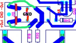
But doing so, if the traces between R19,20,30,40 and the relays are cut, how can the relays shunt to ground the outputs in mute mode? If the relays input not exist (cutting traces) nothing can be shunted to ground.
Let me know your opinion.
Many thanks. Best regards.
Davide.
spzzzzkt said:If the pins are left on and soldered to the pads - which are grounded, it's a simple matter of cutting the traces between R19,20,30,40 and the relays, then running short jumper wires from the relay side of R19,20,30,40 to the output pads. In normal operation the relay is not connected, but in mute mode the outputs are shunted to ground.
[/B]
Hello Paul,
I am looking at your upgrade to the output relays.
But doing so, if the traces between R19,20,30,40 and the relays are cut, how can the relays shunt to ground the outputs in mute mode? If the relays input not exist (cutting traces) nothing can be shunted to ground.
Let me know your opinion.
Many thanks. Best regards.
Davide.
You are right - the "mod" doesn't work as advertised :\
Checking the datasheet for the relay I can see why, and you are 100% correct that as described it won't shunt to gnd. I'd suggest leaving as standard unless you feel like trying out a different method
What I think should work is:
- leaving the connection from the resistors to relay in place.
- cut traces between relay and output connector
- Jumper between "input" pins on the relay and the output connectors
- Tie the "unconnected" pins to GND. If you have trimmed the leads as described in the build notes then you'd need to replace the relays so it's probably not worth the effort in this case.
Attachments
spzzzzkt said:.....unless you feel like trying out a different method
What I think should work is: ........
Hello Paul,
perfect, this is exactly what I was meaning!
Surely in future I will have need of your help and to know your opinion again.
Many thanks in advance. Sincerely
Greetings.
Davide.
My final mods
Firstly, thanks to Spencer for providing the boards and parts to build this DAC.
With the mods described here, the performance of this DAC has gone from "good" to extraordinary! The DAC is now better than my reference THETA Gen Va (which was also modded).
In addition to the mods I mentioned above, I have carried out the following, thanks to HERB (PAOFU).
1. The transport (THETA DATA III) has a 16.xxx MHz clock which I have now fed directly to the digital filter (SM5842). This means that the DAC now does not have to depend on the dirty clock that is recovered from the digital receiver (CS8412). This mod became even better when the THETA's clock was replaced with a low jitter GUIDO TENT clock.
2. I then used flipflops (74HCxxx) to reclock the DATA, WORD and CLOCK signals before they entered the DA converter chips (PCM63PK).
Spzzzzkt provided valuable input here as I tried different experiments.
Performance of the DAC is special, with resolution and presence as strong points. Following these mods, I've put the screws back, perhaps for the first time in about 12 years of tweaking hifi. That says it all!
- Status
- This old topic is closed. If you want to reopen this topic, contact a moderator using the "Report Post" button.
- Home
- Amplifiers
- Pass Labs
- Pass D1V3 DAC - build thread